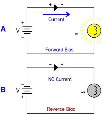
Forward biased diode | Reverse biased diode
Forward bias:
Forward bias definition :
Forward bias: Consider. The positive source terminal is connected to the P-type semiconductor, while the negative source terminal is connected to the N type semiconductor. Here the anode is at higher potential than the cathode. This is called forward biasing.
The battery terminals push holes and free electrons towards the junction. When the battery voltage is less than the barrier potential, the free electrons/holes do not have enough energy to get through the depletion region. When they enter the depletion layer, the ions will push them back. Because of this, no current flows through the diode.
When the source voltage is greater than the barrier potential, the holes and free electrons pushed by the battery terminal have enough energy to cross the depletion region.
The holes in the P-region move to the right and all the free electrons move to the left. Somewhere in the vicinity of the junction, these opposite charges recombine.
The depletion region decreases. The movement of electrons and holes constitute a large current flow through the diode. Obviously, it offers low resistance in the forward direction.
Thus a forward bias voltage equal to barrier potential must be applied across the P-N junction to start the flow of current. This voltage is known as threshold voltage or cut-in voltage or knee voltage. It is about 0.7 V for Si junction and 0.2 V for Ge junction.
ii. Reverse bias:
Reverse bias definition :
When the negative battery terminal is connected to the p side, and the positive battery terminal to the N-side, the P-N junction is said to be connected in reverse bias. Here cathode is at higher potential than anode
The negative battery terminal attracts the holes and the positive battery terminal attracts the free electrons. Because of this, holes and free electrons flow away from the junction.
Therefore, the depletion region widens. Since there is no electron-hole combination inside the P-N region, no current flows and the junction offers high resistance. But in practice, there is a small amount of current flow across the junction due to the flow of minority carriers. As explained earlier, there are always minority carriers present in the semiconductors, viz holes in the N-type region and electrons in the P-type region because of thermal energy.
The applied voltage acts as a forward bias for these minority carriers. The battery drives these minority carriers across the junction thereby producing a small current called as reverse saturation current, Is or lo
Since minority carriers are thermally generated, I, depends on temperature and is independent of reverse voltage.
It is normally of the order of for Ge and nA for Si. Thus in most applications the reverse current in a silicon diode is so small that you do not even notice it.
How to test diode in laboratory? Identify the terminals anode and cathode of the diode.
- Turn the dial (rotary switch) to Diode Test mode . In this mode multimeter supplies a current of 2mA approximately between the test leads.
- Connect the red probe to the anode and black probe to the cathode. This means diode is forward-biased.
- If the displayed voltage value is in between 0.6 to 0.7 (for silicon diode) or 0.25 to 0.3 (for Ge diode) then the diode is working.
- Now reverse the terminals of the meter that means connect the red probe to cathode and black to anode. This is the reverse biased condition of the diode where no curren flows through it.
- Hence the meter should read OL (which is equivalent to open circuit) if diode is working. If the meter shows irrelevant values to the above two conditions, then the diode is defective. The diode defect can be either open or short.
forward bias and reverse bias diagram
Frequently Asked Questions
1. How do contact potential and the transition region width across a P-N junction vary with forward biased?
Answer:
Transition region width is reduced when the P-N junction is forward biased and with an increase in the applied bias voltage the contact potential is reduced.
2. What kind of charges present on the opposite face of the junction?
Answer:
At P side of the junction, negative charges are present and at N side of the junction, positive charges are present.
3. A space region in P-N junction is called the depletion region. Give a reason?
Answer:
During the formation of P-N junction, the space around the junction is completely ionized. Due to this reason, there are no free holes in the P region and no free electrons in the N region. As the area around the junction is drained from mobile charges, it is called the depletion zone.
4. A depletion zone of P-N junction produces electricity. Give a reason?
Answer:
Segregating the densities of positive and negative space charges in a p-n junction results in an electric field.
5. What is the main requirement to forward bias diode?
Answer:
The current is allowed to pass through the PN junction in forward bias mode if the negative side of the supply voltage is connected to the n side of the diode and the supply voltage positive side is connected to the p side of the diode.
6.What is the possible types of biasing ?
Answer:
The three possible types of biasing conditions are as follows:
Forward Bias: This bias condition incorporates the connecting of a positive voltage potential to the P-type material and a negative to the N-type material across the diode, thus decreasing the width of the diode.
Reverse Bias: In contrast, this biasing condition involves the connection of a negative voltage potential to the P-type material and a positive to the N-type material across the diode, thus increasing the width of the diode.
Zero Bias: This is a bias condition in which there is no external voltage potential applied to the diode.
Forward biased diode | Reverse biased diode
Tags:
Basic Electronic System


