Light Emitting Diode (LED) | Use of light emitting diode
Light Emitting Diode Circuit Symbol and Construction
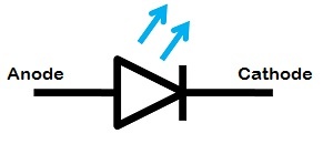
LED is nothing but a single P-N junction diode which emits light when forward biased. The circuit symbol. The outward arrow symbolizes the radiated light.
LEDs play very important role in the field of opto-electronics. LEDs that produce visible radiation are useful in instruments, calculators and so on for display purposes.

The infrared LED finds applications in burglar alarm systems, CD players and other devices requiring invisible radiation. Along with photodiode it is used as an optical isolator. LED forms a potential light source for optical fiber communication.-15
Light Emitting Diode Semiconductor Devices
For the fabrication of LED Si and Ge semiconductors cannot be used. It needs, direct semiconductors like gallium, arsenic, phosphorus. Different materials radiate light of specific wavelength and therefore radiate different colour. The material composition of LEDs required for emission of different colours are given below:
The surface layer is P-type. Therefore a shallow P-N junction is formed and electrical contacts are made to both regions while leaving maximum upper surface of the P-material uncovered so that the radiation from the device is impeded as little as possible.
The junction is encapsulated in transparent plastic medium. The plastic is moulded into an approximate hemishperical shape. Other geometries are also possible which improves the light emission direction and conversion efficiency from electrical to optical.-15
Light Emitting Diode Operating Principle
7.2 Operating Principle
As opposed to other diodes that give off heat when forward biased, LEDs emit light. Emission of light is obtained by injecting carriers into the region of a P-N junction where radiative transition takes place.Thus, emitted light comes from the hole electron recombinations.
For this electrons should make a transition from higher energy level to lower energy level and then release photons of wavelength corresponding to the energy difference associated with this transition. For LED the energy is provided by forward biasing the diode, thus injecting electrons into the N-region and holes into P-region as shown in figure1-18/ Vis
Light Emitting Diode Semoonductor Devices
In forward bias condition, majority carriers from both sides of the junction cross the potential barrier and enter the opposite side where they are then minority carriers. Thus population of minority carriers increase than normal. These excess minority carrier diffuse away from the junction and recombine with majority carriers resulting emission of photon.
Under reverse bias no carrier injection takes place and consequently no photon (light) is emitted.
The forward characteristic is same as rectifying diode except for change in forward voltage drop. the forward characteristics for several LED materials. 8.1 Circuit Symbol and Construction
Photodiode is another opto-electronic device whose reverse current changes with illumination. The construction and symbol of photodiode . The arrows in the symbol represent the incoming light.
The package of the photodiode is transparent so that the light can reach P-N junction. A lens is used in the package to focus maximum light on the junction. The active diameter of device is about 2.5 mm. One side of P-N junction is lightly doped, so that depletion region widens and large area is available for illumination.8.1 Circuit Symbol and Construction
Photodiode is another opto-electronic device whose reverse current changes with illumination. The construction and symbol of photodiode The arrows in the symbol represent the incoming light.
The package of the photodiode is transparent so that the light can reach P-N junction. A lens is used in the package to focus maximum light on the junction. The active diameter of device is about 2.5 mm.
One side of P-N junction is lightly doped, so that depletion region widens and large area is available for illumination.8.1 Circuit Symbol and Construction .Photodiode is another opto-electronic device whose reverse current changes with illumination. The construction and symbol of photodiode . The arrows in the symbol represent the incoming light.
The package of the photodiode is transparent so that the light can reach P-N junction. A lens is used in the package to focus maximum light on the junction. The active diameter of device is about 2.5 mm. One side of P-N junction is lightly doped, so that depletion region widens and large area is available for illumination.
Although colour of light is determined by the material used, the amount of light produced by an LED is controlled by its driving circuit and increases rapidly as current density increases. It is seen from the characteristic that knee voltage for the red LED is the lowest and it increases for shorter wavelength materials.
use of light emitting diode
LEDs used in Dimming of Lights
- Few LED applications include dimming of lights which helps in reducing energy consumption.
- This dimming feature is also used in Appliances where it is of two types.
- Global Dimming where all LEDs are dimmed together.
- Local Dimming where LEDs are dimmed independently.
Light Emitting Diode | Use of light emitting diode
organic leds
the light emitting diode is
organic light emitting diode
light emitting diode is
use of light emitting diode
a light emitting diode is
Tags:
Basic Electronic System


